Introduction
To have a more hands-on experience with my FPGA designs I wanted to connect a keyboard over PS/2 to my iCEBreaker FPGA board. The only problem: The logic-level of the FPGAs IOs are 3.3V and the one of the keyboard are 5V. Therefore I needed a bidirectional levelshifter.
For the PS/2 connector breakout I bought the "Pmod PS2: Keyboard / Mouse Connector" from Digilent.
I have uploaded the design files to this repository.
Working Principle
So how does it work?
Well a single bidirectional levelshifter consists of one MOSFET and two pull-up resistors.
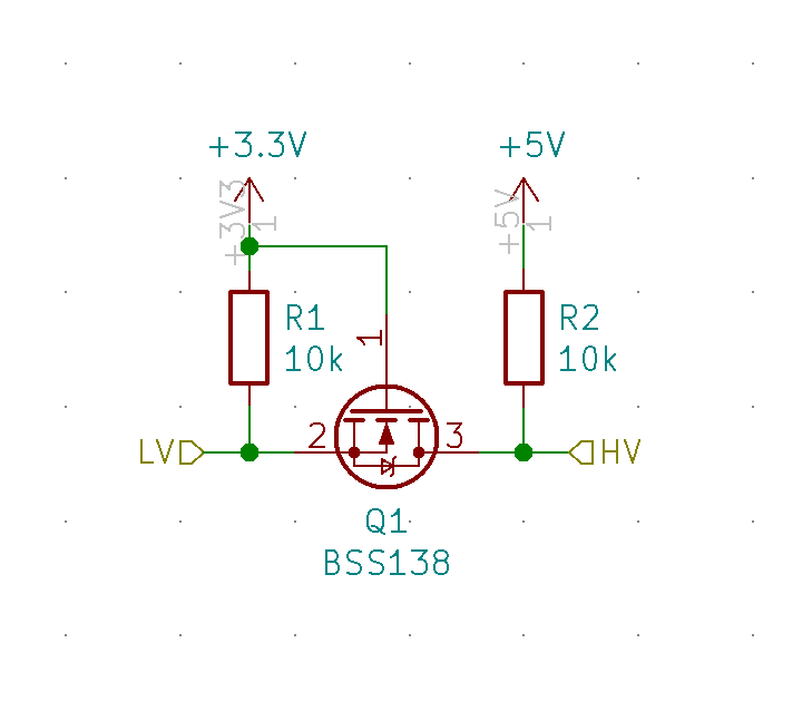
Let's say our LV is 3.3V and the HV is 5V.
Initial state
Now what happens if we do nothing? This means neither the HV or the LV side is pulled down?
Both pull-up registers pull up their corresponding line. The gate and source of the MOSFET are both at 3.3V thus the V_GS is at zero and the MOSFET is non-conducting.
Consequently by default both lines are pulled up to their respective voltage level.
Driving the LV side
Pulling the LV line high wouldn't change anything as this is already done by the pull-up resistor. Now the only thing we can do at the LV side is pulling it low.
What happens then?
With 3.3V at the gate and 0V at the source, the MOSFETs V_GS is at 3.3V which is higher than the threshold. This means the MOSFET becomes conductive. Due to the conducting MOSFET the HV side is also pulled down.
This is exactly what we want, a low level is propagated from LV to HV.
Driving the HV side
Now the other way around: What happens if the HV side is pulled low?
Well, don't forget about the drain-substrate diode. Due to the diode the LV section is pulled down until V_GS passes the threshold and the MOSFET becomes conducting. Now the LV side is pulled to low and stays at this level.
This means that a low level on the HV side is propagated through to the LV side.
Hence we have a bidirectional levelshifter.
PCB Design
I designed the PCB with a Pmod header on one edge and a Pmod socket on the other. Now I can just plug it in between the FPGA and the PS/2 pmod.
Schematic
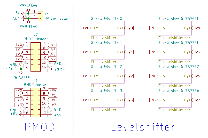
The schematic mainly consists of two parts: the connectors and the MOSFETs. I used hierarchical schematics in this design to keep everything tidy.
PCB
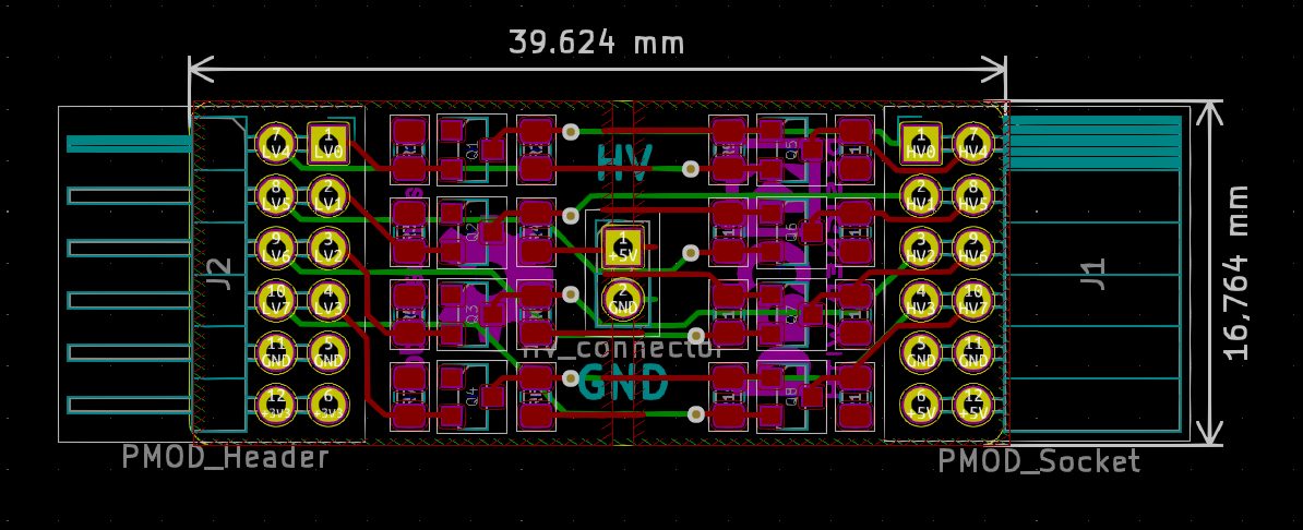
The layout was pretty straightforward. To speed up the placement I used the array feature: You select some components and then they are repeated horizontally and/or vertically x times with a certain distance in between.
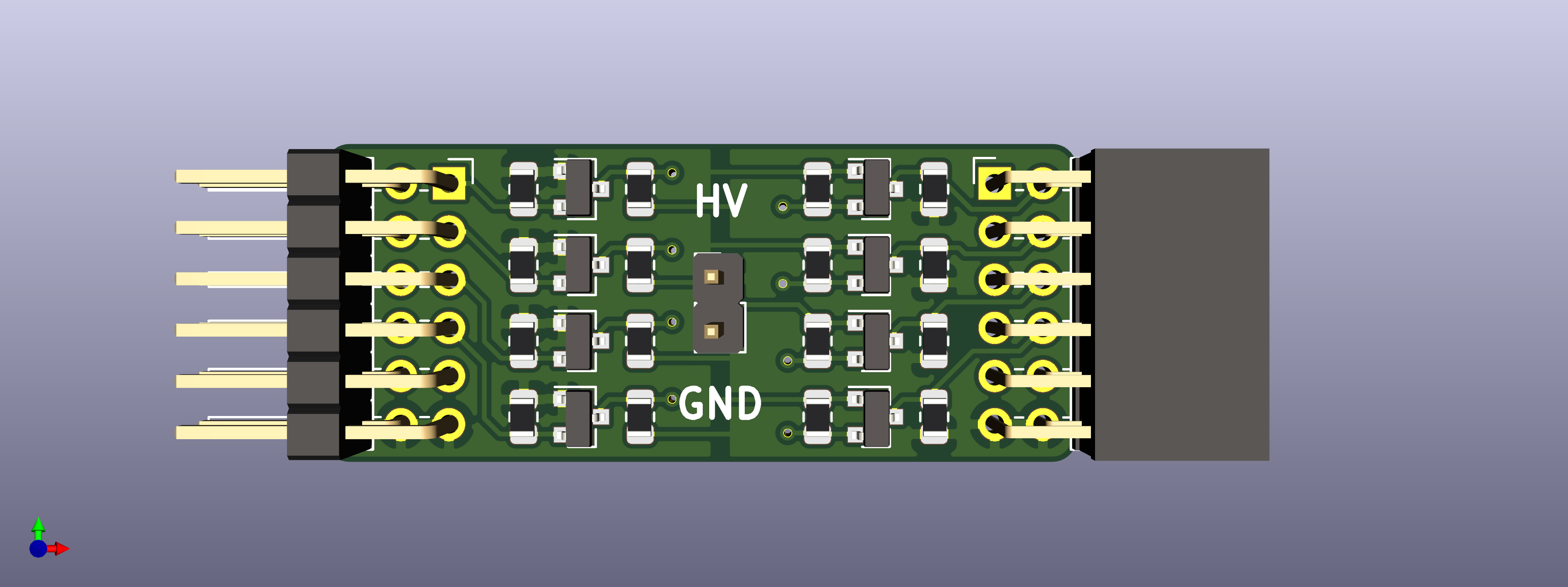
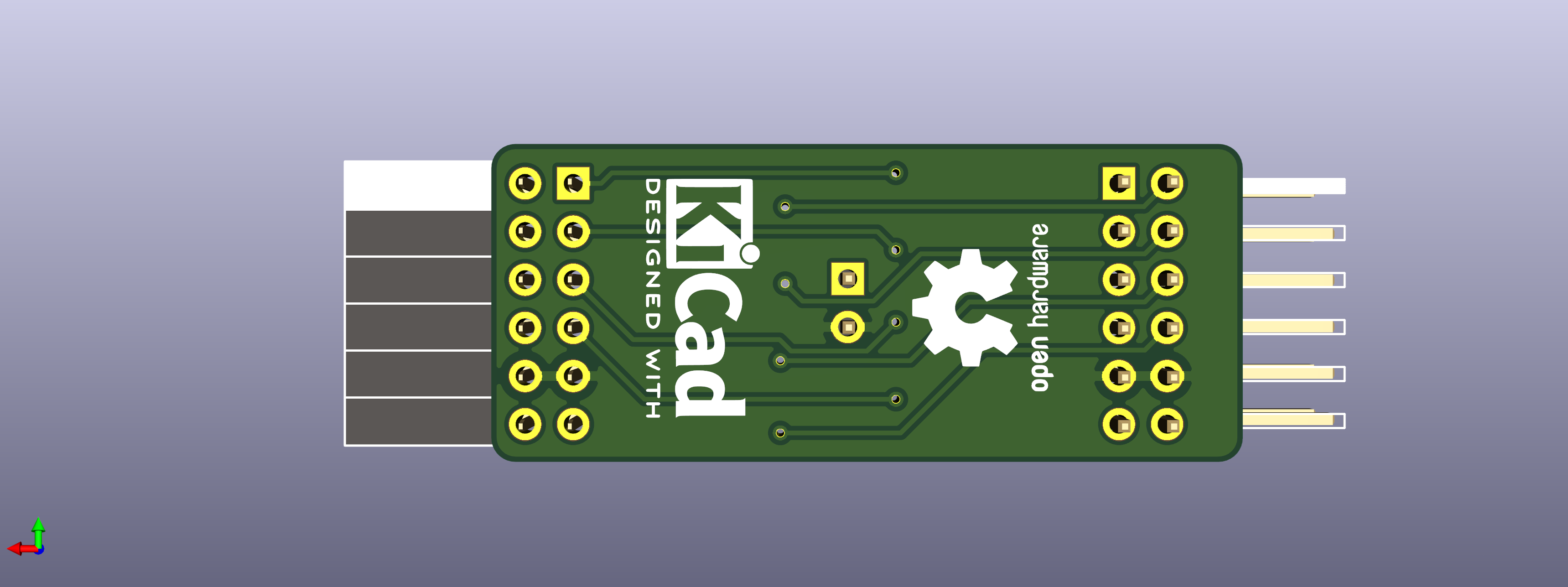
Completed Design
Here are some 3D renders of the completed board.
Next up is soldering the board on my DIY reflow plate.